|
User's
Guide
|
| Home | Prefer the Original? |
New EdSim51SH |
About
the Simulator |
Installation Instructions |
Examples | Contact Us |
The
Fundamental Simulations |
Site Map |
|
||||||||||||||||||||||||||||||||||||||||||||||||||||||||||||||||||||||||||||||||||||


 |
|
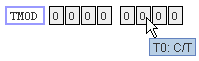 |
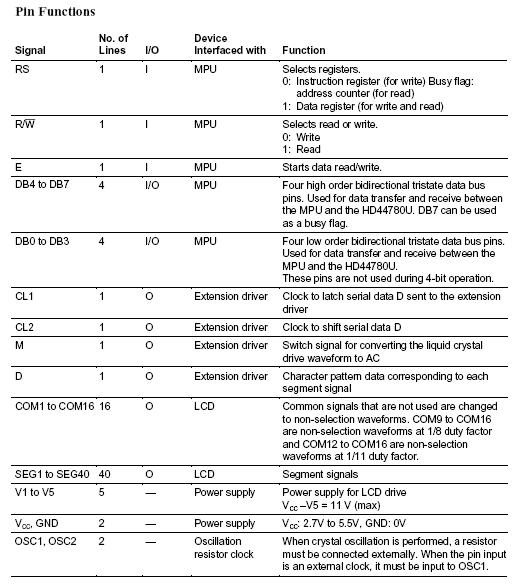
The bit field for the TMOD SFR is shown. Notice bit 2 is the counter/timer bit. Also notice the background is grey. This is because the TMOD register is not bit-addressable - the user cannot alter these bits directly. | |
 |
The PSW is bit-addressable, therefore the background of each bit is white and the user can change any of the bits directly. | |
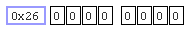 |
The bitfield can be used to see the bit pattern of any address in RAM (0 to 7FH) by typing the address in the blue box. If the location is bit-addressable, the bit backgrounds are white and the user can alter any of the eight bits. | |
 |
As with SFRs, if the location is not bit-addressable the backgrounds are grey. |
|
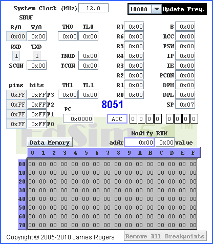
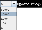
The update frequency may be changed while a user's program is running. |
 |
 |
|
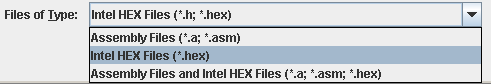
There are two file types handled. The first is plain-text. Assembly programs are saved as regular plain-text files (often called text-only) and usually with .a or .asm file extension. By default, this is the format used when saving your source code in the EdSim51 Simulator.
| The other file type is Intel HEX. The user can select
to save a file in HEX format by choosing Intel HEX
Files from the Files of Type: menu in the Save dialog box. Find out more on loading and saving Intel HEX files. |
 |
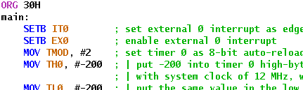
- All of the 8051 instructions are implemented, except for MOVX instructions, as the simulator does not handle external memory.
- JMP rel equates to either SJMP rel or AJMP rel. LJMP rel must be programmed explicitly.
- Similarly, CALL equates to ACALL. LCALL must be programmed explicitly.
- SET and EQU directives are implemented.
- ORG is implemented.
- USING directive (states which register bank is being used) is implemented.
- ARn equates to the register address, as specified by USING (if the register bank is not specified prior to ARn's use, register bank 0 is assumed).
- SFR names and SFR bit names equate to the appropriate address.
- HIGH followed by an operand in brackets equates to the high byte of the operand.
- LOW followed by an operand in brackets equates to the low byte of the operand.
- Labels are followed by a colon.
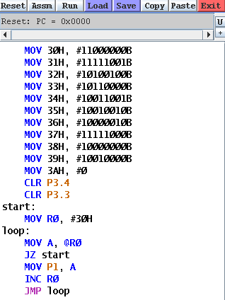
- The default for numerical values is decimal. Hex values can be entered by appending H after the number, or placing 0x before it. If H is used, the number cannot begin with a letter (example: F5H must be written as 0F5H). Binary values are entered by appending B after the number (as shown in the image below).
- The assembler is not case-sensitive.
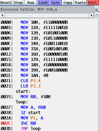 |
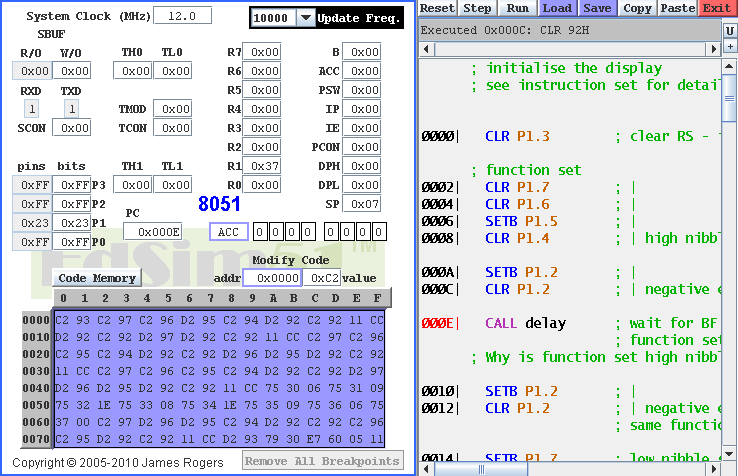
Regardless of whether the code is running or being
stepped, once the code assembles without errors, the address of each
instruction is displayed to the left. When stepping through the code, the instruction that was just executed is shown in the grey box at the top, together with the instruction's address (example shown: Executed 0x2A: MOV 90H, A). The next instruction to be executed, its address is highlighted. (002CH). |
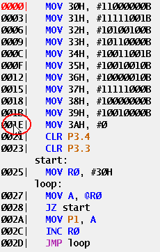 |
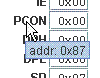
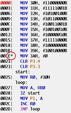
Setting a breakpoint: When stepping through the code, move the mouse over the address of the instruction and double-click. When the breakpoint is set the vertical bar (|) immediately to the right
of the address is replaced by a star (*),
as shown in the image on the right.
Removing a breakpoint: A breakpoint is indicated
by a star (*). To remove
the breakpoint, move the mouse over the instruction's address and
double-click. The * is
replaced by |. Alternatively, you can remove all breakpoints with one
click of: |
 |

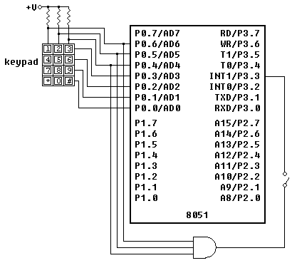
Also, there are instances in the following section where the sharing of port pins is pointed out. For example, the motor and the UART share the same port pins. This of course may not be true in your case, if, for example, you move the motor to other pins.
 |
|
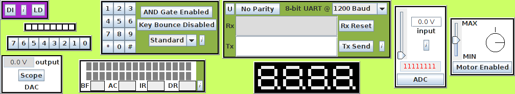
|
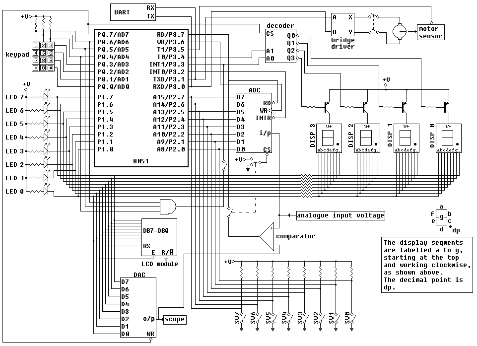
- ADC
- Comparator
- Four 7-segment LED Displays
- LCD Module
- UART
- Keypad
- LED Bank
- Bi-directional Motor
- Switch Bank
- DAC (output displayed on oscilloscope)
 |
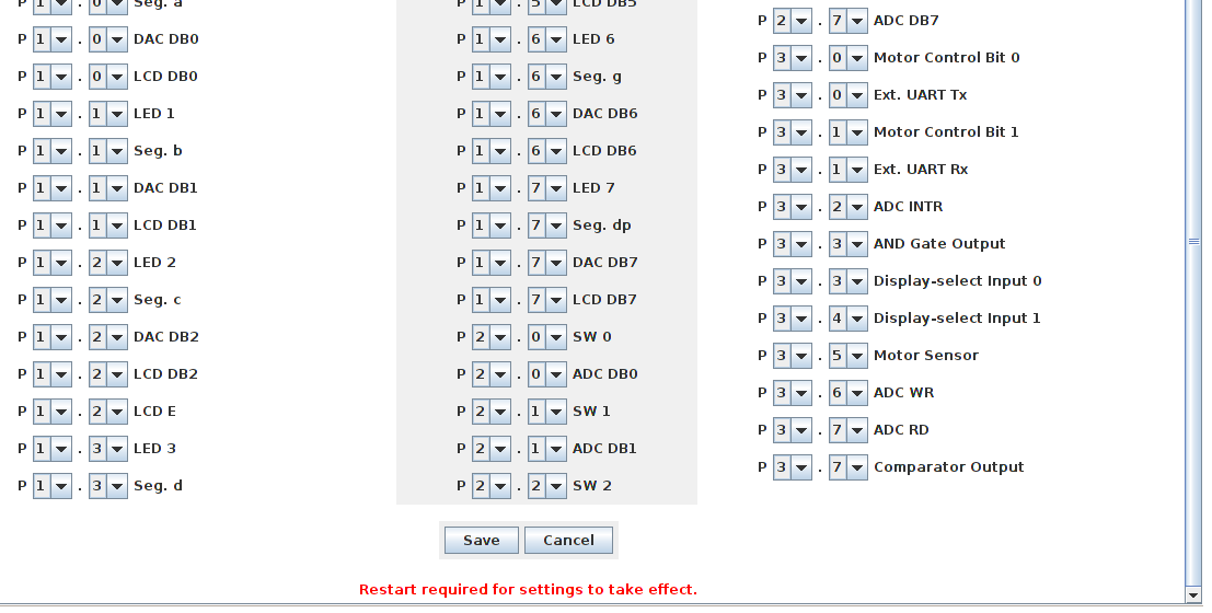
These image on the left shows what is connected to each of the 32 port pins. If a pin's description is too long to fit, you can see the full description by hovering the mouse over it, or by clicking on the zoom button (see below).
Zoom
|
| Port Pin Connections | |
 |
|
|
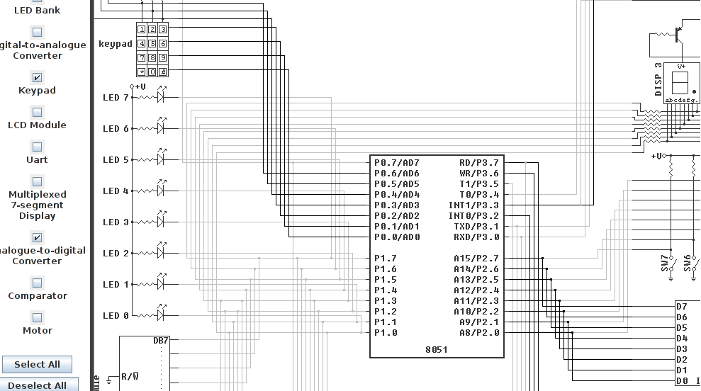
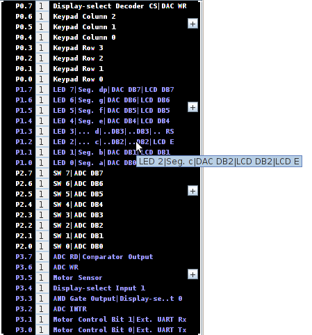
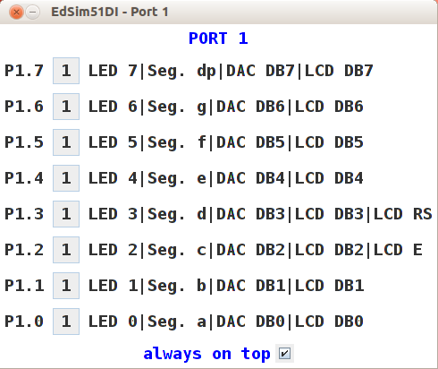
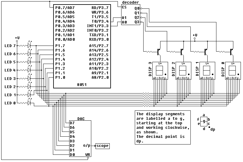
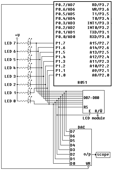
As can be seen in the diagram below, the LED bank, the DAC inputs and the 7-segment display data lines all share port 1.
 |
 |
 |
  |
||
|
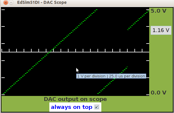
Ramp Generated via DAC
Appears on Scope
|
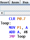
Code for Ramp Generation
|
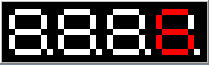
LED Bank and the
7-segment Displays Panel |
When the mouse is placed over the scope screen, a tooltip appears, stating the scope's vertical scale is one volt per division and the horizontal scale is, in this case, 25 microseconds per division. The scope's horizontal scale is tied in with the 8051 system clock frequency (this is unrealistic, but I feel it's adequate for simulation purposes). If, for example, the system clock frequency is changed to 11.059 MHz, then the scope's horizontal scale is 17.36 microseconds per division.
|
|
|
|
 |
The enable pin (E,
connected to P1.2) is negative-edge triggered. On a negative-edge on E,
the module reads the data lines DB7 - DB4. 4-bit Mode: As can be seen in the logic diagram above, the module is interfaced with the 8051 in 4-bit mode. In 4-bit mode, the module's lines DB3, DB2, DB1 and DB0 are not used. The 8-bit instruction or data must therefore be sent in two 4-bit nibbles. The high nibble is sent first, followed by the low nibble. When the enable pin is taken high and then low, this causes the module to read the pins DB7-DB4 and store them in either the IR (if an instruction is being sent - ie: RS = 0) or the DR (if data is being sent - ie: RS = 1). Initially, the module is in 8-bit mode and must be set to 4-bit mode by the programmer before any other communications with the module are attempted. This is done by sending the appropriate Function Set instruction (see instruction set below). Why send Function set twice? As stated, the module is initially in 8-bit mode, therefore the first instruction sent to it is read as an 8-bit instruction (as if DB3 - DB0 were in use). If the correct instruction is sent (with DL - on DB4 - set to zero, indicating 4-bit - see below), then the module 'knows' it is being set to 4-bit operation and it reads instructions and data in two 4-bit nibbles from then on. Because it reads the high nibble first, the Function set high nibble must be sent again, followed by the low nibble. For more information, see pages 39 and 42 of HD44780.pdf. The example on page 42 is for a 1-line display, but it nonetheless explains clearly how to initialise and communicate with the module in 4-bit mode. 8-bit Mode: Even if 8-bit mode is being used, Function set must first be called to ensure the module is set to 2-line with 5 X 8 font. See below. 2-line, 5 X 8 Font: The low nibble of Function set must be sent with N = 1 (setting the number of lines on the display to 2) and F = 0 (setting the font to 5 X 8 dots). |
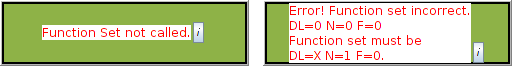 |
Function Set Incorrectly: The programmer must set the module to 2-line, 5 X 8 font. The simulation of the HD44780 is implemented for 2-line, 5 X 8 font only. However, the programmer is still expected to write the code that sets the module in this mode. If the mode is not set correctly, an error message stating such is displayed, as shown here. The programmer must then reset the simulator, modify the code and try again. |
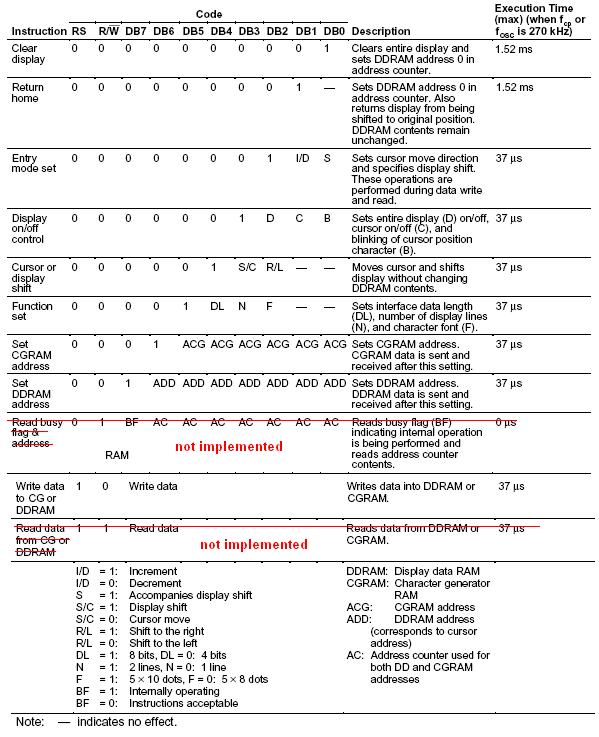
LCD Module Instruction Set
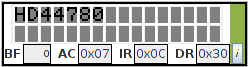
CGRAM stands for character generator RAM. The module's ROM contains the ASCII character set. For example, the ASCII code for the letter W is 87, so stored in location 87 in the module's RAM is the pattern for W. This makes it relatively easy to write text to the display. The following code extract illustrates this point:
MOV A, 'W'
CALL sendCharacter ; a subroutine that sends the data in A to the LCD module's DDRAM
When DDRAM receives a character, the corresponding pattern from ROM is displayed.
Note in the ASCII set, the first seven locations are used for control characters. These characters are not applicable to the LCD module, therefore these locations are reserved for CGRAM instead. When a value in the range 0 to 7 is sent to DDRAM, instead of displaying a character from ROM, the corresponding character from CGRAM is displayed.
This means the user can create eight custom characters. The characters are programmed into CGRAM by pointing to CGRAM (instead of DDRAM) and then sending data to the module the same as when sending data to DDRAM.
If you look at the instruction set above you will see there is a Set CGRAM address instruction. Note the address is six bits in length - we will discuss these six bits shortly.
Also notice there is only one instruction for writing to the module. To write to CGRAM, you must first ensure the AC (address counter) is pointing to CGRAM. You do this by calling the Set CGRAM address instruction. As with writing to DDRAM, the AC is incremented (or decremented, depending on the increment/decrement setting) after each write to CGRAM.
It was mentioned above that ROM contains the ASCII set. This is not altogether true. There are instances where the character in ROM does not correspond with ASCII. At location 92 you would expect to see the \ symbol. Instead there is ¥ (probably because the HD44780 was developed in Japan). At location 126, instead of ~ in location 126 there is a right arrow symbol, followed by a left arrow symbol in location 127.
So, if you want to display the \ symbol, for example, you will first need to create it in CGRAM. You can choose any of the eight CGRAM locations, but let's say we wish to put \ in location 2.
Each character is made up of eight rows, with five dots in each row. You write the pattern for each row to CGRAM, one row at a time. The row's pattern is made up of 1s where dots are to be visible and 0s where dots are to be invisible.
The six CGRAM address bits are split into two parts. The top three bits determine which of the eight CGRAM characters is being written to, while the bottom three bits determine which of the eight rows of this character is being written to.
| CGRAM Character Address (binary) | Row Address (binary) | Value Written to CGRAM | |||||||||||||||||||||||||||||||||||||||||||||||||||||||||||||||||
|
|
|
|
The three character bits and the three row bits make up the 6-bit CGRAM address.
Note that the top row is row 0 while the bottom row is row 7 (111B). You can use the bottom row when creating a custom character, but it is not advisable to do so, especially if you intend using the cursor as well.
The example above shows how to create the \ symbol in CGRAM location 2. You start by setting CGRAM address to 2, then send the pattern for the character's first row to CGRAM (in this case, 00H). The AC will automatically increment to point to the next row. You then send the pattern for that row (in this case, 10H), and so on for all eight rows.
Once completed, you can then display your new character by setting the DDRAM address to some value, then send the number 2 to DDRAM and your new character in CGRAM location 2 will appear on the display.
You might then write a test, as shown below, to ensure the correct symbol is displayed when writing \ to the LCD:
... ; data to be sent to LCD has been placed in A
CJNE A, #'\', skip ; if A does not contain \ symbol, skip next line
MOV A, #2 ; replace \ with location of \ in CGRAM
skip: CALL sendCharacter ; call the subroutine that sends the contents of A to the LCD
For complete instructions on how to program the LCD module, see HD44780.pdf.
|
|
|
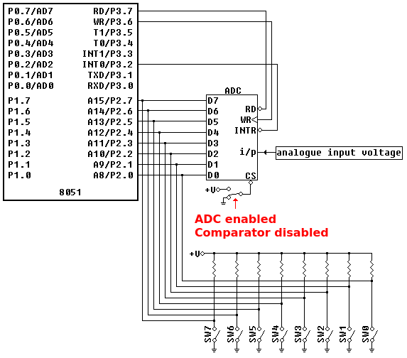
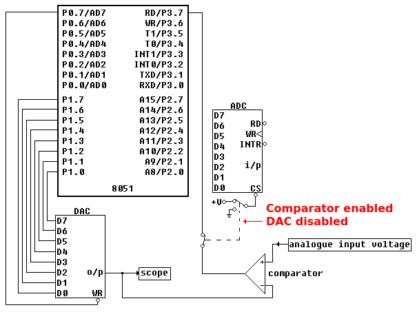
When a switch is open a logic 1 appears on the port pin (via the pull-up resistor) while closing the switch connects the pin directly to ground - logic 0. The switch bank and the outputs of the ADC are applied to port 2. Therefore, it should be noted that when the ADC is being used the switches in the switch bank should all be open (in the simulator, the switches are grey when they are closed). If a switch is closed it doesn't matter what the ADC tries to put on that line, the line is held low because it is connected directly to ground through the closed switch. |
||
| Logic diagram showing the switch bank and ADC connections only. |
 |
The outputs of the ADC are tri-state: the RD line,
which is connected to P3.7, must be low for the ADC reading to appear
on the outputs. The WR line (connected to P3.6) is used to initiate a conversion. As it is positive edge triggered, it must be taken low and then high to start a conversion. When the conversion is complete the INTR line goes low (and remains low until another conversion is initiated). This line is applied to the external 0 interrupt line, INT0. In this way, the 8051 can be interrupted by the completion of an ADC conversion. Note the tip that appears when the mouse is placed over the ADC button. Clicking on this button disables the ADC and enabled the comparator. See the Comparator for more information. |
Pin Function RD Enables the tri-state outputs, when logic 0. WR On a positive edge, initiates conversion. INTR Goes to logic 0 when conversion is complete and remains low until another conversion is initiated. i/p Analogue input signal applied here. CS Enables the device, when logic 0. D0 - D7 Tri-state digital outputs.
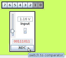
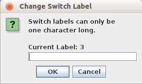
Changing Switch Labels
| You can change the label
of a switch in the switch bank by right-clicking
on the switch and entering a new character. A switch label can only be one character in length. |
 |
|
|
 |
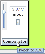 |
The analogue input that is applied to the ADC is also applied to the non-inverting pin of the comparator, as can be seen above (in this extract, since the ADC is disabled, the analogue voltage connection to the ADC is omitted). When the comparator is enabled, the button's label says Comparator, as can be seen in the image opposite. Hovering over the button displays a tip - click the button to disable the comparator and enable the ADC. The button corresponds to the switch at the ADC chip select and the switch between the comparator output and P3.7 in the logic diagram extract above. You can see the switch between the comparator output and P3.7 is closed while at the same time the ADC CS line is switched to +V, disabling the ADC. |
Learn about comparators and DACs used as ADCs (An external site that is not affiliated with EdSim51.)
|
|
|
|
||||||||||||||||||||
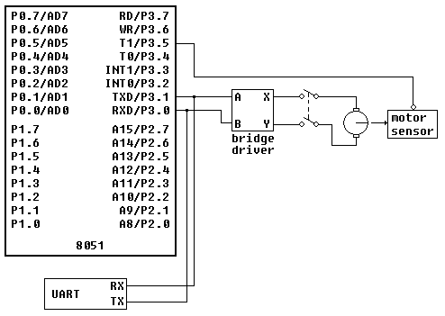
| Logic diagram showing the motor and UART connections only. |
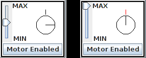 |
In the image on the left, the motor's shaft is in the default position (pointing at 3 o'clock). Notice the sensor (depicted by a vertical line at the top of the motor) is black. When the motor's shaft lines up with the sensor, the sensor changes from black to red, as shown in the image on the right. |
|
|
 |
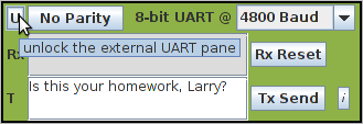
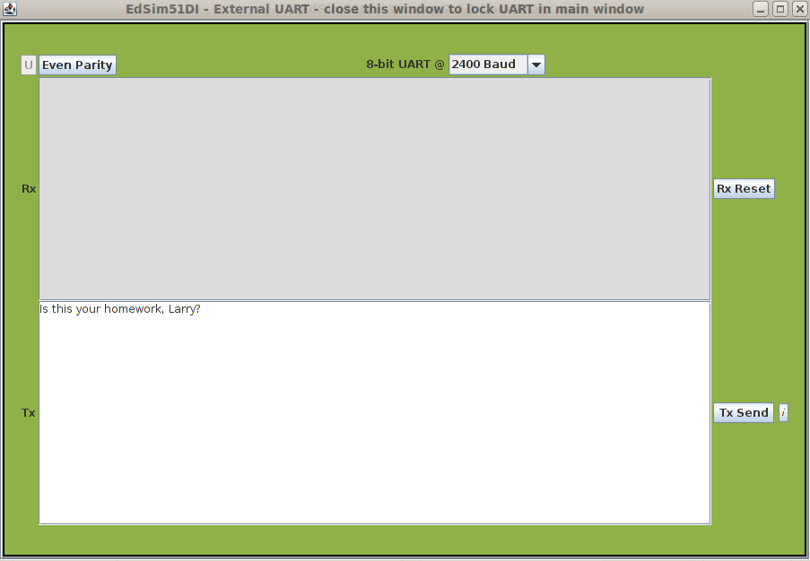
As stated above, the motor control lines share the same port pins as the 8051 serial port RXD and TXD. An external UART is connected to P3.0 and P3.1. Data received from the 8051's serial port appears in the Rx window. The data in this window can be cleared at any time by clicking the Rx Reset button. |
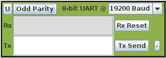
No Parity (the default), Odd Parity and Even Parity.
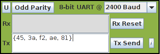 |
Rather than text, a list of 8-bit numbers (written in
HEX) can be transmitted. To do so, the user encloses the list in curly
braces, each number separated by a comma, as shown in the image
opposite. When text is transmitted, it is terminated by 0DH. This is not the case with a list of numbers. In the example shown opposite, the four numbers 56, 3a, 23 and e7 are transmitted, nothing more. |
|
| If the user wishes to send {56, 3a, 23, e7} as text rather than a list of 8-bit numbers, the text is escaped using the \ character. Therefore, \{56, 3a, 23, e7} in the Tx field would result in {56, 3a, 23, e7} followed by 0DH being transmitted to the 8051. | ||
|
|
|
 |
||
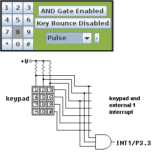
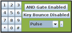
| Logic diagram showing the keypad connections only. |
Key Bounce
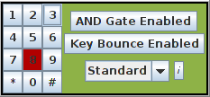 |
If Key Bounce is enabled, as shown in the image opposite, then
the keys will bounce when closed (the keypad only bounces
if the keypad
mode is set to standard). So the user knows a key is
bouncing, its colour alternates between red (switch open) and dark red
(switch closed). Once the switch finishes bouncing, its colour reverts
to dark grey. The length of the switch bounce is 30 ms. Note: a key will only bounce while a program is running. If the user pauses the running program, then the switch bounce also pauses. |
- Standard - in standard mode the keys are independent of each other. Any number of keys can be closed at the same time. A closed key is reopened simply by clicking on it again.
- Pulse - in pulse mode a key is closed while the (left) mouse button is held down. Once the mouse button is released the key reopens.
- Radio - in radio mode only one key at a time can be closed. For example, if key 5 is pressed (ie: closed) and then key 7 is pressed, key 5 automatically reopens. As in standard mode, a closed key is reopened simply by clicking on it again.
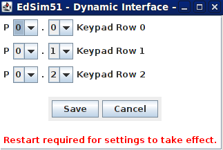
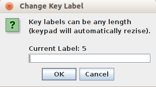
| You can change the label
of a key by right-clicking
on the key and entering a new character. Key labels can be any length. The keypad resizes automatically. |
 |
Original Setting Update Freq. 1 Bitfield Address ACC Data/Code Memory Data Memory File System Directory Operating System Dependent ADC/Comparator Enabled ADC Enabled External UART Parity No Parity External UART Baud Rate 4800 Baud Keypad AND Gate Disabled Keypad Type Standard Key Bounce
No Key Bounce
Key Labels #, 0, *, 9, 8, 7, 6, 5, 4, 3, 2, 1
Switch Labels
0, 1, 2, 3, 4, 5, 6, 7
Motor Enabled/Disabled Enabled
| Home | Prefer the Original? |
New EdSim51SH |
About
the Simulator |
Installation Instructions |
Examples | Contact Us |
The
Fundamental Simulations |
Site Map |